This article explains IGBT, its symbol, construction and working principle with relevant structure and circuit diagrams.
What is IGBT?
IGBT (Insulated Gate Bipolar Transistor) is a three terminal power switch having high input impedance like PMOSFET and low on-state power loss as in BJT (Bipolar Junction Transistor). Thus, IGBT is a combined form of best qualities of both BJT and PMOSFET. This is the most popular power switch among the power-electronics engineers and find a great variety of applications.
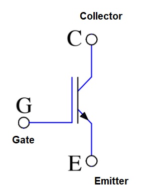
IGBT is a three-terminal device. The three terminals are Gate (G), Emitter (E) and Collector (C). The circuit symbol of IGBT is shown below.
IGBT is also known as metal oxide insulated gate transistor (MOSIGT), conductivity-modulated field effect transistor (COMFET) or gain-modulated FET (GEMFET). It was initially called Insulated Gate Transistor (IGT).
Construction of IGBT:
An IGBT is constructed on a p+ layer substrate. On p+ substrate, a high resistivity n- layer is epitaxially grown. As in other semi-conductor devices, the thickness of n- layer determines the voltage blocking capability of IGBT. On the other side of p+ substrate, a metal layer is deposited to form the Collector (C) terminal. Now, p regions are diffused in the epitaxially grown n- layer. Further, n+ regions are diffused in p region. A basic construction structure of IGBT is shown in figure below.
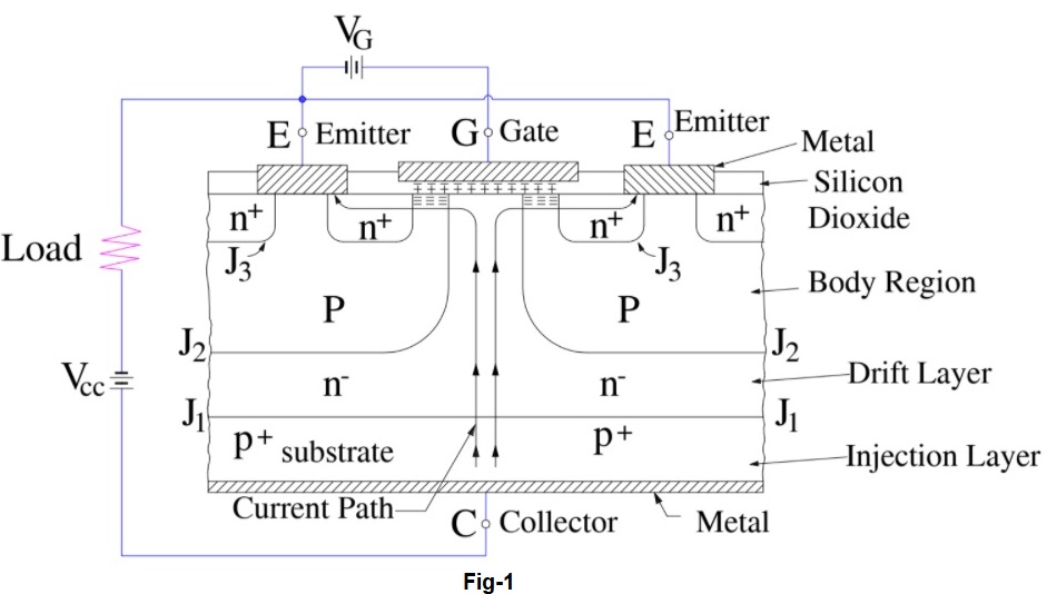
Now, an insulating layer of Silicon Dioxide (SiO2) is grown on the surface. This insulating layer is etched in order to embed metallic Emitter and Gate terminals.
The p+ substrate is also called injector layer because it injects holes into n- layer. The n- layer is called drift region. The next p layer is called the body of IGBT. The n- layer in between the p+ & p region serves to accommodate the depletion layer of pn- junction i.e. J2.
Equivalent Circuit:
The approximate equivalent circuit of IGBT comprises of MOSFET and p+n-p transistor (Q1). To account for resistance offered by the n- drift region, resistance Rd has been incorporated in the circuit. This is shown below.
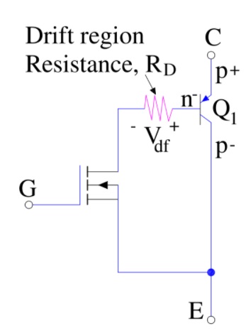
This equivalent circuit may be arrived at by a careful examination of basic structure of IGBT. The basic structure is shown below.
From the above figure, it is clear that as we move vertically up from collector to emitter, we come across p+, n-, p layers. This means that IGBT can be thought of as the combination of MOSFET and p+n–p transistor (Q1). This is the basis for approximate equivalent circuit.
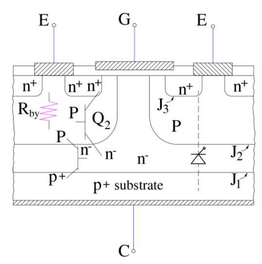
Now, carefully observe the basic structure of IGBT shown above. You will notice that there exists another path from collector to emitter; this path is collector, p+, n–, p (n-channel), n+ and emitter. There is, thus, another transistor Q2 as n–pn+ in the structure of IGBT. Thus, we need to incorporate this transistor Q2 in the approximate equivalent circuit to get the exact equivalent circuit.
The exact equivalent circuit of IGBT is shown below.
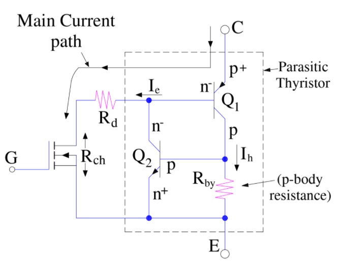
Rby in this circuit is the resistance offered by p region to the flow of hole current.
Working Principle of IGBT:
The working principle of IGBT is based on the biasing of Gate to Emitter terminals and Collector to Emitter terminals. When collector is made positive with respect to emitter, IGBT gets forward biased. With no voltage between Gate and Emitter, two junctions between n- region & p region i.e. junction J2 are reversed biased. Therefore, no current flows from collector to emitter. You may refer figure-1 for better understanding.
When Gate is made positive with respect to Emitter by some voltage VG (this voltage should be more than the threshold voltage VGET of IGBT), an n-channel is formed in the upper part of the p-region just beneath the Gate. This n-channel is called the inversion layer. This n-channel short circuits the n- region with n+ emitter region. Electrons from n+ emitter begins to flow to n- drift region through n-channel.
As IGBT is forward biased with collector positive and emitter negative, p+ collector region injects holes into n- drift region. Thus, n- drift region is flooded with electrons from p-body region and holes from p+ collector region. With this, the injection carrier density in n- drift region increases considerably and subsequently, conductivity of n- region enhances. Therefore, IGBT gets turned ON and begins to conduct forward current IC.
Current IC or IE comprises of two current components:
- Hole current Ih due to injection of holes from collector p+, p+n–p transistor Q1, p-body region resistance Rby and emitter.
- Electronic current Ie due to injected electrons flowing from collector, injection layer p+, drift region n-, n-channel resistance Rch, n+ and emitter.
Therefore, the collector, or load current
IC = Emitter Current
= IE
= Ih + Ie
Major current of collector current is electronic current Ie i.e. main current path for collector, or load, current is through p+, n-, drift resistance Rd and n-channel resistance Rch. This is shown in exact equivalent circuit.
The voltage drops in an IGBT during its ON condition consists of voltage drop in n-channel, voltage drop across drift n- region, voltage drop across forward biased p+n- junction J1. The voltage drop across junction J1 is very small of the order of 0.7 to 1V. The ON state voltage drop of IGBT is very small and hence ON state losses are also low.
After applying positive voltage to gate with respect to emitter it will attract the electron from p region(body) as emitter and p(body) region at same potential (Zero) similar to working of MOSFET. But How gate will attract the electron from n- region(drift) as collector voltage is more positive than gate voltage?
To put in nut shell my question is
Is there any contribution from n-(drift) region to form N-Channel below the gate??
Actually n-(drift) region acts as Drain terminal (for the MOSFET counterpart of the IGBT) while P (body region) acts like Substrate (for the same MOSFET counterpart of the IGBT). Because it is the substrate where the action of gate electric field acted upon, so there is no question of n-(drift) region (-the Drain terminal as mentioned above) to take part in inducting the n channel beneath Gate mentalised region.
upload charecrtstics