Switching Characteristics of IGBT is basically the graphical representation of behavior of IGBT during its turn-on & turn-off process.
The turn-on time is defined as the time between the instant of forward blocking to forward conduction mode. Here, forward conduction means the device conducts in forward direction. Turn-on time (ton) is basically composed of two different times: Delay time (tdn) and Rise time (tr). Therefore, we can say that ton = tdn + tr.
The delay time is defined as the time for the collector-emitter voltage (VCE) to fall from VCE to 0.9VCE. This simply means that, the collector-emitter voltage drops to 90% in delay time and hence the collector current rises from initial leakage current to 0.1IC (10%). Thus, delay time may also be defined as the time period during which collector current rises from zero (in fact a small leakage current) to 10% of the final value of collector current IC.
The rise time tr is the time during which collector-emitter voltage falls from 0.9VCE to 0.1 VCE. This means, during rise time collector-emitter voltage falls to 10% from 90%. Therefore, the collector current builds up to final value of collector current IC from 10%. After time ton, the collector current becomes IC and the collector-emitter voltage drops to very small value called conduction drop (VCES).
A typical Switching Characteristics of an IGBT is shown below. You may corelate the delay time, rise time and turn-on time.
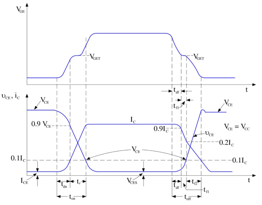
Let us now focus on turn-off time. Unlike turn-on time, turn-off time comprises of three intervals:
- Delay Time, tdf
- Initial Fall Time, tf1
- Final Fall Time, tf2
Thus, turn-off time is the sum of above three different time intervals i.e. toff = tdf + tf1 + tf2. Kindly refer the switching characteristics of IGBT for interpretation of above times.
The delay time is the time during which gate voltage falls from VGE to threshold voltage VGET. As gate voltage falls to VGE during tdf, the collector current falls from IC to 0.9IC. At the end of delay time, collector-emitter voltage begins to rise.
The first fall time tf1 is defined as the time during which collector current falls from 90% to 20% of its final value IC. In other words, it is the time during which collector-emitter voltage rises from VCES to 0.1VCE.
The final fall time tf2 is the time during which collector current falls from 20% to 10% of IC or the time during which collector-emitter voltage rises from 0.1VCE to final value VCE.
Thanks for this switching characteristics
Great Article. An IGBT is a semiconductor with three stations that work as a switch for moving electrical current. An IGBT will switch the present on and off so rapidly that less voltage will be channeled to the motor, selecting to create the pulse width modulation wave.
Thank you for bringing such topic into light, I really loved the concept of your article. Thanks for sharing this information. It’s a great source of knowledge; I think it will be helpful for lot of people who are looking for learning more about switching characteristics of igbt.