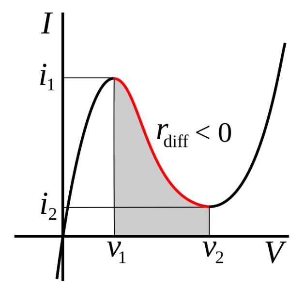
A tunnel diode is a diode that exhibits a negative differential impedance region in its I-V characteristic due to quantum tunneling effects. That is, a -sloped region as shown by red colored region in the figure below.
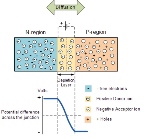
It’s a diode, a kind of semiconductor device usually with two terminals. Unlike a regular pn diode, Tunnel Diode conducts both ways. This is due to a peculiarity of the manufacturing process in which the impurity i.e. dopant concentration is intentionally high, that the semiconductor becomes a bit more like a conductor having small resistance.
Semiconductors are the only materials that exhibit this weird behavior. If we add impurities in a metal, it won’t significantly alter its resistance.
Heavy doping in Tunnel Diode is intentional, because it alters the energy levels in the semiconductor. This allows such that the engineered gap between the p and n material types to be much larger than normal.
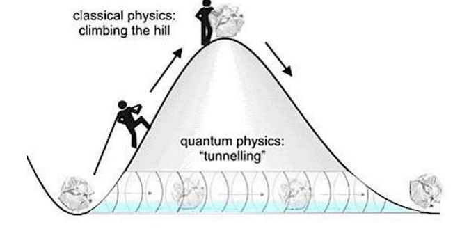
The above effect makes it very convenient for electrons to move and they are not allowed to jump from the lower energy level to the higher energy just like that; what happens here is quantum tunnelling, an effect where modern physics shows that electrons teleport through thin wall as shown in figure below.
Therefore in short,
Tunnel diode is a highly doped semiconductor device and is used mainly for low voltage high frequency switching applications. It works on the principle of Tunneling effect. It is also called as Esaki diode named after Leo Esaki, who in 1973 received the Nobel Prize in Physics for discovering the electron tunneling effect used in these diodes.
Thank you!