This article explains Single Phase Full Bridge Inverter with the help of circuit diagram and various relevant waveforms. Comparison between half and full bridge inverters have also been detailed.
Single Phase Full Bridge Inverter is basically a voltage source inverter. Unlike Single Phase Half Bridge Inverter, this inverter does not require three wire DC input supply. Rather, two wire DC input power source suffices the requirement. The output frequency can be controlled by controlling the turn ON and turn OFF time of the thyristors.
Circuit Diagram of Single Phase Full Bridge Inverter:
The power circuit of a single phase full bridge inverter comprises of four thyristors T1 to T4, four diodes D1 to D1 and a two wire DC input power source Vs. Each diode is connected in antiparallel to the thyristors viz. D1 is connected in anti-parallel to T1 and so on. The power circuit diagram of a single phase full bridge inverter is shown in the figure below.
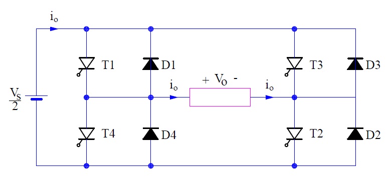
It may be noted that the circuitry for turning ON and turning OFF the thyristor is not shown in the above circuit diagram to maintain simplicity. Further, it is assumed that each of the thyristor only conducts for the period its gate signal is present and as soon as the gate signal is removed, the thyristors gets turned OFF.
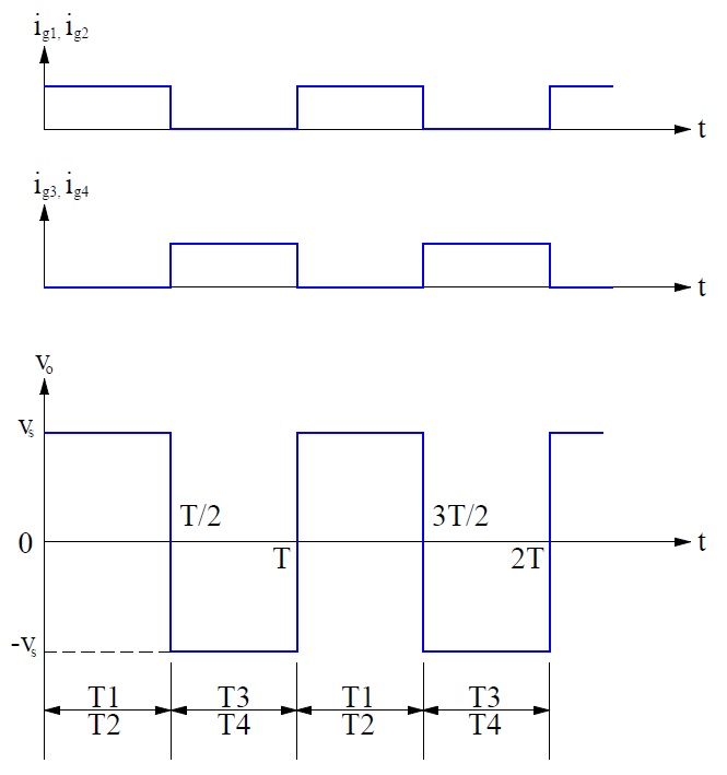
The gating signal and output voltage waveform of a single phase full bridge inverter is shown below.
Working Principle of Single Phase Full Bridge Inverter:
The working principle of single phase full bridge inverter is based on the sequential triggering of thyristors placed diagonally opposite. This means, for half of time period, thyristors T3 & T4 will be triggered while for the remaining half of time period, T1 & T2 will be triggered. Only two thyristors are turned ON in half of the time period.
Carefully observe the waveform of the gating signal. You will notice that thyristors T1 & T2 are triggered simultaneously for a time T/2. Therefore, load is connected to source through T1 & T2 and hence, the load voltage is equal to the source voltage with positive polarity. This is the reason; the load voltage is shown positive & equal to Vs in the output voltage waveform.
As soon as the gate signal (ig1 & ig2) are removed, T1 and T2 gest turned OFF. However, at the same instant gate signal (ig3 & ig4) are applied and hence, T3 & T4 are turned ON. When T3 & T4 are conducting, load gets connected to the source. The load voltage magnitude is again Vs but with reverse polarity. This is the reason, the output voltage is shown negative in the voltage waveform.
To summarize,
For the time 0<t≤(T/2), thyristors T1 & T2 conducts and load voltage Vo = Vs.
For the time (T/2)<t≤T, thyristors T3 & T4 conducts and load voltage Vo = -Vs.
I think you have understood the working principle of single-phase half bridge inverter. But I am sure that you might be thinking the purpose of diodes D1 to D4. I will explain.
Purpose of Diodes D1 to D4:
If the load is purely resistive, there is no need to put diode D1 to D4 as the output voltage and current are always in phase. But unfortunately, for loads other than purely resistive, the load current (io) will not be in phase with the load voltage (vo). For such case, the diode connected in anti-parallel with the thyristor will allow the current to flow when main thyristor is turned off. When these diode conducts, the energy is fed back to the DC source and hence, these diodes (D1 to D4) are called flyback diode.
Comparison between Half & Full Bridge Inverters:
The major difference between the single phase half and full bridge inverter is that former requires a three wire DC input source while the latter requires two wire DC source. Another difference between the two type of inverters are tabulated below:
| Half Bridge Inverter | Full Bridge Inverter |
| It comprises of two thyristors and two free-wheeling diodes. | It consists of four thyristors and four flyback diodes. |
| The magnitude of load / output voltage is half of the magnitude of input DC source. | The magnitude of load voltage is equal to the magnitude of DC input source. This means, the magnitude of output voltage is twice the magnitude of load voltage for half bridge inverter. |
| The main drawback of this inverter is the requirement of three wire DC input supply. | This drawback of half bridge inverter is overcome by full bridge inverter as it requires two wire DC source. |
| – | The output power of full bridge inverter is four times that of for half bridge inverter. |
very excellent explanation.
thanks a lot
Thank you! Kindly share.
I have not understand why the thyristors turn off once they are turned on.
I mean SCR can be controlled only in one direction, so once we apply the gate signal the turning off happens once there is a voltage reverse (as for diodes). So, once we trigger T1 and T2, how do they turn off? Where is the voltage inversion stopping the SCR to be conducting?
Thank for your attention and for the reply
How do you drive the high-side ‘thyristors’ that are placed above the load?
In my requirement, Vs = 50V and I wasn’t able to find a suitable gate driver IC that accept a Vs of 50V (most ICs top out at 20-25V for ‘supply voltage’).
Am I reading their datasheets wrong? Would you be able to suggest a suitable gate driver IC?
Sorry I meant LOW-side ‘thyristor’ that is placed BELOW the load.
My Vs is 50V.
D1 to D1
It should be D1 to D4 in Circuit Diagram of Single Phase Full Bridge Inverter