This article outlines the basic operating or working principle of a Single Phase Half Bridge Inverter with the help of circuit diagram.
Single Phase Half Bridge Inverter is a type of Single-Phase Bridge Inverter. It is a voltage source inverter. Voltage source inverter means that the input power of the inverter is a DC voltage Source. Basically, there are two different type of bridge inverters: Single Phase Half Bridge Inverter and Single-Phase Full Bridge Inverter.
As the input power source is DC, there is no meaning of single phase with respect to input power. However, it does have a meaning with reference to output. The output of single-phase bridge inverter is a single-phase output. Let us now discuss the basic operating or working principle of Single-Phase Half Bridge Inverter.
Working Principle of Single-Phase Half Bridge Inverter:
The working / operating principle of half bridge inverter is based on the fact that, for half of time period of output wave, one thyristor conducts whereas for another half of time period, another thyristor conducts. The output frequency of this type of inverter may be controlled by controlling the switch ON and switching OFF time of thyristors. Figure below shows the power circuit diagram of a single-phase half bridge inverter.
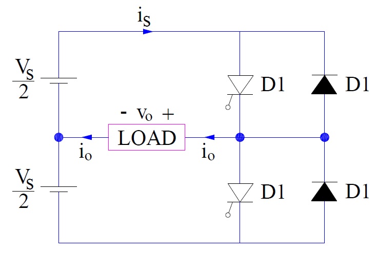
Single Phase Half Bridge Inverter comprises of two thyristors T1 & T2, two diodes D1 & D2 and three wire DC source. The circuit for turning ON and turning OFF the thyristor is not shown in the above circuit to maintain simplicity. While analyzing the circuit, it is assumed that each thyristor conducts for the duration its gate pulse is present and is commutated as soon as this pulse is removed. The gating signal for thyristor T1 (ig1) and thyristor T2 (ig2) and output voltage waveform of this inverter is shown below.
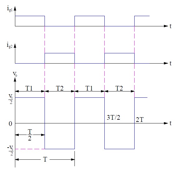
Carefully observe the gating signal for T1 & T2. It can be seen that ig1 is applied for a period of 0<t≤(T/2), this means thyristor T1 will conduct for this time period. During the time T1 conducts, load is directly connected to source (Vs/2) on the upper arm. Thus, the load voltage / output voltage will be equal to the input source voltage (Vs/2) for 0<t≤(T/2).
As soon as ig1 is removed at t= T/2, thyristor T1 gets turned OFF. It may be seen from the waveform of gating signal that at t=T/2, ig2 is applied and hence, thyristor T2 gets turned ON. Thus, load gets directly connected to the source (Vs/2) on the lower arm. Note that the polarity of voltage source on the upper & lower arm are opposite to each other. Therefore, during the time (T/2)<t≤T, T2 is ON, the output voltage is -(Vs/2) as shown in the output voltage waveform.
It may also be seen form the output voltage waveform that load voltage is an alternating square voltage waveform of amplitude (Vs/2) and frequency (1/T) Hz. Thus, output frequency can be controlled by controlling T.
I think you have understood the working principle of half bridge inverter. But I am sure that you might be thinking the purpose of diodes D1 & D2. I will explain.
Purpose of Diodes in Half Bridge Inverter:
If the load is purely resistive, there is no need to put diode D1 & D2 as the output voltage and current are always in phase. But unfortunately, for loads other than purely resistive, the load current (io) will not be in phase with the load voltage (vo). For such case, the diode connected in anti-parallel with the thyristor will allow the current to flow when main thyristor is turned off. When these diode conducts, the energy is fed back to the DC source and hence, these diodes (D1 & D2) are called flyback diode.
Drawbacks:
The main drawback of single phase half bridge inverter is that it requires 3-wire DC supply source. However, this drawback can be overcome by the use of full bridge inverter.