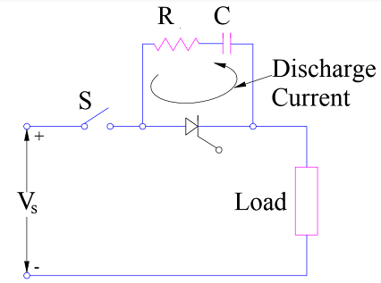
Snubber Circuit is a circuit consisting of series combination of resistance and capacitance in parallel with SCR. This article describes the purpose, design and working principle of Snubber Circuit in detail.
Purpose of Snubber Circuit
The main purpose of Snubber Circuit is to prevent the unwanted triggering of SCR or thyristor due to high rate of rise of voltage i.e. dv/dt. We already know that if the rate of rise of anode to cathode voltage of SCR is high then it may lead to false triggering. This is commonly known as dv/dt triggering. Thus we need to have some arrangement to protect SCR from such undesirable turning. Application of Snubber Circuit prevents from such spurious triggering of SCR. Thus it is basically dv/dt protection of SCR.
Design and Working Principle of Snubber Circuit
As we need to limit the rate of rise of anode to cathode voltage of SCR during its turn on process, this means we should use a capacitor the SCR terminals. Why? This is because a capacitor limits the rate of rise of voltage whereas an inductor limits the rate of rise of current. Thus a capacitor when connected across the SCR terminals, when limit dv/dt. Lets us now connect the capacitor across the SCR terminals and see how this affects the dv/dt.

As you can see, we have connected capacitor C in parallel with SCR. When switch S is closed, a sudden voltage appears across the circuit. Initially capacitor C behaves like a shorted path and hence the voltage across SCR is zero. But as time passes, voltage starts building up across capacitor C with a slow rate. Thus the rate of rise of voltage dv/dt across SCR terminals will also be slow and less than the specified dv/dt rating of SCR.
But the above circuit design has one problem. Let us go deep into the above circuit to make improvement. As you can see, before SCR is fired or triggered by applying gate pulse, the capacitor C is fully charged up to supply voltage Vs. As soon as SCR is turned on by gate pulse, this charged capacitor C discharges through SCR. Hence a current having magnitude (Vs/Resistance of loop formed by SCR and Capacitor C) flows in the local path formed by SCR and capacitor C. Since the value of resistance of this local path is quite small, the magnitude of discharge current will be quite higher. This will lead to high value of di/dt which may exceed the specified di/dt rating of SCR. In order to limit the magnitude of the discharge current, a resistance should be connected in series with the capacitor C. This is shown below.

The above circuit is the actual Snubber Circuit. Thus, a snubber circuit comprises of series combination of resistance and capacitance in parallel with SCR or thyristor. Generally, resistance R, capacitance C and load parameters are so chosen that the dv/dt during charging of capacitor C is less than the specified dv/dt rating of SCR and the discharge current at the turn on of SCR is less than the specified di/dt rating. Normally, R, C and load parameter forms an underdamped circuit so that dv/dt is limited to acceptable value as provided by the SCR rating.
In the above circuit if capacitor acts as short circuit then the current reached to the load at the initial stage of switching on the circuit ? Then how to control the load current?
Capacitors only act as a low impedance (or short-circuit) when AC is applied to them and the value of the cap is high. In the above drawing, DC is applied so the the capacitor only needs to charge one time, upon the closing of the switch. Because the cap is of such a low value, the current through the load to charge the cap will be negligible compared to the power required by the load.