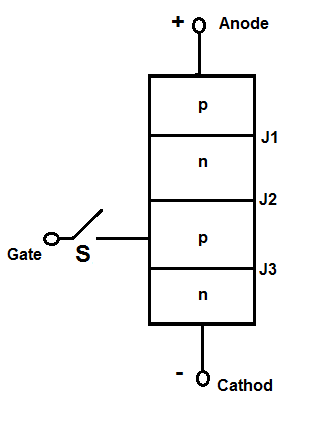
Switching characteristics of SCR is the time variation of voltage across its anode and cathode terminals and the current through it during its turn on and turn off process. This means, there will be two types of characteristics: One during turn on process and other during turn off process of SCR. It is also known as dynamic characteristics of SCR. In this article first we will be discussing the switching characteristics during turn on and then for turn off process of SCR. Delay time, Rise Time and Spread Time associated with SCR Tun On process and Reverse Recovery Time and Gate Recovery Time associated with SCR Turn Off process has also been explained in detail.
Switching Characteristics of SCR during Turn On
We are already aware that of the fact that, an SCR starts conducting when it is forward biased and gated pulse is applied. This means, when we apply gate pulse, SCR changes its state from Forward Blocking Mode to Forward Conduction Mode. But the point which should be thought of that, does SCR immediately jumps to Forward Conduction Mode when we apply gate pulse or there is some transition time? In fact, there is a transition time from forward off state to forward on state. This transition time is called SCR or thyristor turn on time.
SCR or Thyristor Turn on Time
Thyristor turn on time may be defined as the time required by the SCR to change its state from forward blocking mode to forward conduction mode when a gate pulse is applied. The total turn on time of SCR comprises of three different time intervals: Delay Time, Rise Time and Spread Time.
Delay Time:
The delay time is measured from the instant at which gate current reaches to 0.9Ig to the instant at which anode current reaches 0.1Ia. Here Ig and Ia are the final values of gate and anode current respectively.
There are various other ways to define delay time. It is also defined as the time during which anode voltage falls from Va to 0.9Va. Here Va is the initial value of anode to cathode voltage when SCR was in forward blocking mode. Another way to define it is the time in which anode current reaches to 0.1Ia from forward leakage current.
The initiation of turn on process basically starts at gate to cathode junction. As soon as we apply gate current, charges are injected into the gate to cathode junction. This charge initially flows in a narrow path due to non-uniform charge distribution. Therefore the current density near the gate is more and decreases as the distance from gate junction increases. This means, during delay time the anode current flows in a narrow region near gate where gate current density is higher.
Rise Time:
Rise time is defined as the time taken by the anode current to rise from 0.1Ia to 0.9Ia. During this time, the anode to cathode voltage drops from 0.9Va to 0.1Va. Rise time is inversely proportional to the magnitude of gate current and its rate of rise. The more the value of gate current, the lesser will be the rise time.
During rise time, the current starts to spread from a narrow conducting region in the gate to cathode junction. But as the rise time is small, the anodes current do not get a change to spread over the entire cross section of cathode. Thus we can say that, like in delay time, the current during rise time also flows in a narrow region. However the area of this narrow region is more than that in case of delay time.
Since the current and voltage are more during rise time, the turn on losses in SCR is more during rise time.
Spread Time:
Spread time of SCR or thyristor is time taken by anode current to reach from 0.9Ia to Ia. During this time period, the anode current spreads over the entire cross section of cathode. After the spread time, the anode current attains a steady state value and the voltage drop across the SCR terminals becomes equal to on stage voltage drop of the order of 1 to 1.5 V.
From the above discussion, we observe that an SCR is a charge controlled device during turn. This is also evident from the fact that, a certain amount of charge is injected by the gate current in the gate to cathode junction to bring the SCR in forward conduction mode from its forward blocking state. This means, the higher the value of gate current, the lesser will be the turn on time. In general, the magnitude of gate current to turn on SCR is about 3 to 5 times the minimum gate current required to trigger SCR. When the gate current is several times higher than the minimum gate current required, an SCR is said to be hard fired or overdriven SCR.
Switching Characteristics of SCR during Turn Off
Switching Characteristics of SCR during Turn Off is the transition of SCR from forward conduction state to forward blocking state. This transition process involves bringing the anode current below holding current, sweeping out of charges from outer p and n junction and recombination of holes and electrons at the interior junction. Thus it is a dynamic process. This dynamic process of bringing SCR to off state is called commutation process or turn off process. Let us discuss, switching characteristics of SCR during turn off in detail.
As we know that, once SCR is turned on, gate has no control over it. This means, the SCR will continue to be in conduction state even if gate current is removed. Ok, but now we want to turn off SCR. So what we need to do? We need to bring the anode current below holding current. But merely bringing anode current below holding current won’t turn off SCR. This is because the charge carriers i.e. electrons and holes are still in favorable condition and if we apply forward voltage across anode and cathode terminals, SCR will begin to conduct. This means, we need to apply a reverse voltage for some finite time to give charge carries time to be swept away from outer p and n junction due to reverse voltage. Once the charge has been swept away and recombined in inner junction where sweeping is not possible, the SCR will sustain forward voltage. At time stage, we will say that SCR is turned off. This whole process takes some time, which is known as turn off time of SCR.
Turn off time (tq) is defined as the time in between the instant when anode current becomes zero to the instant when SCR regains forward blocking capability. During this time, all the excess carries from outer p and n layers are removed as discussed above. This removal of excess carriers consists of sweeping out of holes from outer p-layer and electrons from outer n-layers. The carriers in the inner junction can only be swept away by recombination. Thus there are two different methods for sweeping out excess carriers. This lead to two different times. The time in which excess carriers are removed from two outer p and n layer is called Reverse Recovery Time trr. While the time in which carriers in inner layer is removed due to recombination is called the Gate Recovery Time, tgr.
Figure below shows the switching characteristics of SCR during turn on and turn off process.
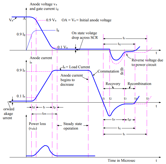
Following points can be noted with reference to above switching characteristics of SCR during turn off process:
- At instant t1, the anode current becomes zero. But carriers are still under favorable condition, the anode current will start flowing in reverse direction with the same slope i.e. di/dt. This is actually good. This reverse current will help to sweep out excess holes from outer p-layer and excess holes from outer n-layer. This reverse current first increases but with the sweeping out of excess carriers, this current starts to decrease. At time t2, when around 60 percent of carriers have been swept away from outer layers, the reverse anode current stars to decrease. The rate of decay of reverse current fast in the beginning but becomes gradual thereafter. This fast decay of reverse current cause a reverse voltage across the SCR or thyristor terminals and may therefore damage it. An RC element across SCR terminal helps to protect from such type of happening.
- At time t3, when reverse current becomes almost zero, the excess carriers have been completely removed and now the SCR can withstand the reverse voltage.
- The reverse recovery time is, therefore, (t3 – t1).

- After reverse recovery time trr, the excess carries are still trapped in the inner junction J2. Therefore, the SCR is not able to block the forward voltage. Since the excess charge around junction J2 is not able to flow in the external circuit, therefore these trapped charges must decay due to recombination. This recombination is only possible if a reverse voltage is maintained across SCR for some finite time, though the magnitude of this reverse voltage is not important. This is because; the rate of recombination only depends on junction temperature. It is independent of external circuit parameter. The time for recombination of charge is called Gate Recovery Time, tgr. Here the gate recovery time is (t4 – t3).
- At instant t4, as there is no excess charge, the SCR can withstand forward voltage. Hence we say that SCR has turned off. SCR or thyristor turn off time is in the range of 3-100 µs.
- The SCR turn off time depends on the magnitude of anode current prior to starting of commutation process, di/dt and junction temperature. An increase in magnitude of these factors, increases the thyristor turn off time. However, turn off time decreases with increase in magnitude of reverse voltage. This is because; high reverse voltage quickly sweeps out holes from outer p-layer and electrons from outer n-layers. Thus turn off time of SCR is not a constant parameter of thyristor, rather it is depends on the external circuit parameter.
- SCR forms a part of external circuit. The turn off time provided to the SCR or thyristor by the practical circuit is called Circuit Turn off Time, tc. It is defined as the time between the instant anode current becomes zero to the instant reverse voltage across SCR terminals becomes zero. Circuit turn off time tc must be greater than thyristor turn off time tq for reliable commutation.
Thyristors with slow turn off time (50-100 µs) is called converter grade SCR and those with fast turn off time (3-50 µs) is called inverter grade SCR. Converter grade SCRs are cheaper and used for Phase Controlled Rectifiers, AC Voltage Controllers etc. Inverter grade SCRs are costlier and used for Chopper, Inverter and forced commutated converters.
Excellent service