A pn junction diode is a two terminal single crystal semiconductor device whose one side is doped with acceptors and other side by donors. Doping with acceptor creates p type semiconductor while doping with donors produces n type. Thus a pn junction is formed in diode.
The formation of pn junction in a single crystal due to doping with p type and n type material is shown in figure below.
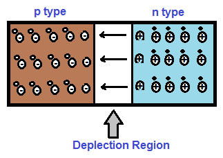
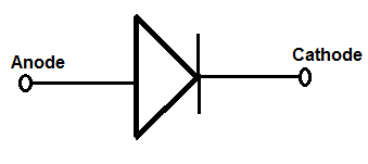
In the above figure, left side of crystal is p type while the right side is n type. The positively charged donor ions in n type is shown by encircled plus sign while negatively charge acceptor ions are shown by encircled minus sign. The circuit symbol of pn junction diode is shown below.
Working Principle of pn Junction Diode
The working principle of a pn junction diode can be broadly understood under three categories: Unbiased pn Junction, Forward Biased pn Junction and Reversed Biased pn Junction. We will discuss each of them one by one.
Unbiased pn Junction Diode
Unbiasing means, no voltage source is connected across the terminals of pn junction diode. Let us investigate the phenomena happening inside the junction.
Since p side and n side is having holes and electrons as the majority carrier, the concentration of hole is more in p side whereas concentration of electron is more in n side. Due to this difference in concentration, holes will start to diffuse toward the n side and electrons will start to diffuse toward p side. In this process, holes and electrons will recombine and hence will neutralize. As a result, the acceptor ions near the p side and donor ions near the n side are left un-neutralized. This un-neutralized ion near the vicinity of pn junction is called uncovered charges. The positive and negative uncovered charge produces an electric field across the pn junction. The direction of this electric field is from n side to p side. This electric field set up by the uncovered charges in the pn junction diode is called the Barrier Field. This barrier field opposes the diffusion of holes and electrons and equilibrium is reached when the strength of this barrier field is enough to stop further diffusion of holes and electrons across the pn junction. After this, there will not be any further diffusion of majority carriers. Thus the neighborhood of junction is devoid of any free charges and therefore this region of pn junction is called the Depletion Region. The terms depletion itself means that there is a depletion of free charges in the region i.e. pn junction.
The potential difference between the pn junction is called the Barrier Potential. The main reason for generation of barrier potential is charge separation due to diffusion process. This leads to production of barrier field and hence associated barrier potential. The value of this barrier potential is dependent on the semiconductor, doping and width of depletion region. The more the width of depletion region, the more will be the barrier potential.
Due to this barrier potential, work needs to be done for bring a hole from p side to n side. Similar is the case for electron. If barrier potential is assumed to be VB, then the work required to be carried out for bringing a hole from p side to n side will be equal to eVB. Thus we observe that there exists a barrier potential across the pn junction of diode. So we must be able to measure this by using voltmeter? If you ever try to measure this voltage by connecting the lead of voltmeter across the diode terminals, you will get zero reading. Isn’t it a contradiction? It is true that there exists a barrier potential, but at the same time it is also true that there exists a contact voltage drop between the semiconductor and metal contact. The barrier potential is exactly balanced by the contact potential at the metal-semiconductor contacts at the ends of diode terminals. This is the reason, the voltmeter is unable to measure the barrier potential of diode.
To summarize, there is no flow of current in an unbiased pj junction diode. It is just a device under this condition.
Forward Biased pn Junction Diode
A pn junction diode is said to be forward biased if the positive plate of battery is connected to the p side and negative plate to the n side. A forward biased diode is shown in figure below.
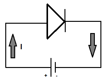
Since p and n sides are connected to positive & negative plate of battery respectively, the positive plate will force the holes in p side toward n side and attract the electrons in n side toward p side. Similarly, the negative plate will push the electrons in n side and will attract the holes in p side. Thus both the positive and negative plates are exerting a force for the flow of holes and electrons. If the battery voltage is more than the barrier potential, the holes and electrons will have enough energy to cross the pn junction. Subsequently flow of current will start through the pn junction diode. It should also be noted that the width of depletion region will decrease under forward biased condition. Thus in forward biased diode, current flows from anode to cathode or from p side to n side as shown in above figure.
To summarize, a forward biased diode acts like a closed switch provided the forward biasing voltage must be greater than the barrier potential. If the forward biasing voltage is less than the barrier potential, the energy imparted by battery to the electrons and holes will not be enough energy to cross the pn junction. Hence it will block the flow of current. Thus we observe that a diode not a bilateral device. Note that bilateral device is once which allows the flow of current in both the direction.
Reverse Biased pn Junction Diode
A pn junction diode is said to be reverse biased if the positive plate of battery is connected to the n side and negative plate to the p side. A reverse biased diode is shown in figure below.
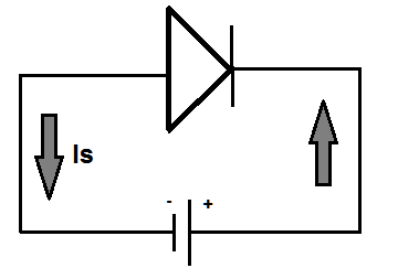
Under reverse biased condition, the width of depletion region increases as the battery voltage pulls the holes in p side and electrons in n side away from the junction. Thus there will not be any flow of holes and electrons across the junction. Subsequently, there will not any flow of current through the pn junction diode.
But the flow of minority carrier i.e. electrons in p side and holes in n side remain unaffected. It should be noted that the concentration of minority carrier is dependent on the temperature. These are thermally generated minority carrier in p and n side. Due to flow of minority carrier across the junction, a small current flows from cathode to anode. This current is called Reverse Saturation Current. Value of reverse saturation current is independent of reverse bias voltage but dependent on junction temperature. Its value increases with increase in junction temperature. The flow of reverse saturation current Is is shown in above figure.
A reverse biased pn junction diode acts like an open switch and blocks the flow of current from anode to cathode.
Points To Remember
- A forward biased pn junction diode acts like a closed switch provided the forward biasing voltage must be greater than its barrier potential.
- The width of depletion region decreases with increase in forward bias.
- A reverse biased diode do not conduct and hence acts like an open switch.
- The width of depletion region increases with increase of reverse bias voltage.
- A small reverse current flows from n side to p side in a reversed biased pn junction diode or simply diode. This current is called Reverse Saturation Current.
- The value of reverse saturation current is independent of reverse bias voltage. Its value depend on the junction temperature. The higher the junction temperature, the more will be the value of reverse saturation current.