Avalanche Breakdown is the process of current carrier multiplication due to collision of thermally generated minority carriers with crystal ions in a lightly doped reverse biased pn junction diode. An avalanche of current carriers is produced in a very short time due to this breakdown of pn junction diode. Holes in n side and electrons in p side are minority carriers. Current carriers in pn junction diode are holes and electrons.
A reverse biased pn junction diode is one whose n side is connected to positive battery terminal whereas p side is connected with negative battery terminal. With increase in reverse bias voltage the electric field across the junction increases. At a certain value of reverse bias voltage, the electric filed imparts sufficient energy to the thermally generated minority carriers (holes in n side & electrons in p side are minority carrier) present in the p side and n side.
Due to this imparted energy, these carriers are accelerated across the pn junction and attain enough kinetic energy. These carriers when collides with the semiconductor crystal ions on its way, ruptures the covalent bond to produce a new electron hole pair. These newly born electron hole pair may again get accelerated by the electric filed and may rupture another covalent bond to produce new electron hole pairs. Thus a single minority carrier produces two new current carriers i.e. one electron and one hole. This means, there are a total of three current carriers (1 electron+1 pair of newly generated electron and hole). This process is cumulative and can produce a large number of current carriers within a very short time. This cumulative process of production of current carrier due to collision of minority carrier with semiconductor crystal ion is called Avalanche Breakdown.
Avalanche breakdown is mostly observed in lightly doped pn junction diode. In highly doped pn junction diode, zener breakdown is observed.
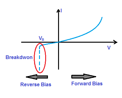
Avalanche breakdown results in avalanche of current carriers in the diode. The movement of these carriers under the effect of applied reverse voltage causes a flow of higher current in the reverse direction. What is mean by reverse direction? Normally current through diode flows from Anode to Cathode but in this condition the direction of current is from Cathode to Anode. Figure below shows the region of avalanche breakdown in the V-I characteristic of diode.

From the above V-I characteristics, it is can be seen that until the reverse bias voltage is less than a certain value (VB), a small amount of reverse saturation current flows in the reverse direction. But as soon as this reverse bias voltage reaches VB, the current suddenly increase. This is shown by dashed line in the V-I Characteristics. This voltage VB at which breakdown of diode take place is known as breakdown voltage.
The value of this breakdown voltage varies for avalanche as well as zener breakdown. Generally, avalanche breakdown voltage is more than 5 V while it is less than 5 V for zener breakdown. You might think why don’t then zener breakdown occurs first as its value is less than avalanche breakdown voltage. This is because zener breakdown take place in highly doped pn junction diode. In lightly doped diode, avalanche breakdown will take place when the reverse bias voltage exceeds 5 V.
A diode designed to operate in breakdown region is called breakdown diode. These diodes must have sufficient power dissipation capacity as the value of current in breakdown region is quite high.