A Center Tapped Full wave Rectifier is a circuit which makes unidirectional flow of current through the load during the full cycle of input voltage. Two diodes are so connected across the terminals of center tapped transformer secondary terminals that one diode conducts for positive half cycle and another diode conduct for negative half cycle of the supply input. Thus a unidirectional flow of current is maintained through the load resistance. Since, a center tapped transformer is used for the rectification purpose, this is called center tapped full wave rectifier.
This is basically an improvement over half wave rectifier in which output current only flows for the positive half cycle of input supply. Figure below shows a circuit diagram of the center tapped full wave rectifier.
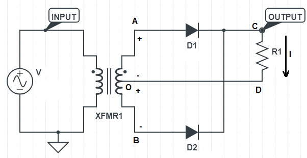
In the above circuit, XFMR1 is the center tapped transformer and D1&D2 are two identical diodes. Note the word identical. It is very important to have the same characteristics of both the diode used in the rectifier circuit to minimize the ripple. R is the load resistance.
Let us now understand the working of center tapped full wave rectifier.
Working of Center Tapped Full Wave Rectifier
For the positive half cycle of the supply input V, the polarity of XFMR1 secondary terminal A will be positive with respect to center point O. At the same instant, the polarity of terminal B will be negative with respect to center point O. This means, for positive half cycle of the supply input, diode D1 will be forward biased and D2 will be reverse biased. Hence D1 will conduct for this period while D2 won’t. Thus current through load will flows from C to D due to conduction of D1.
Similarly for the negative half cycle of input supply V, diode D1 will be reverse biased and D2 will be forward biased. This means for this period, D2 will conduct and D1 will not conduct. This will result in flow of current through the load resistance R from C to D.
Thus, we see that, current flow through the load is maintained from C to D for positive as well as negative half cycle of the supply voltage. Or we can say that, a unidirectional flow of current is maintained through load.
Figure below shows a result of simulation of the center tapped full wave rectifier.
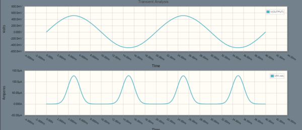
You are requested to zoom above simulation result and carefully observe the following:
- The load current is flowing for positive as well as negative half cycle of the supply voltage.
- The diode is not conducting until the supply voltage crosses around 360 mV. This is due to the cut-in voltage requirement of diode. Basically, a forward biased diode can only start conduction if its forward biasing voltage exceeds cut-in voltage. This is the reason, diodes D1 & D2 are not conducting for around 2 ms in the beginning when supply voltage starts from zero and crosses 360 mV and 2ms at the end when supply voltage drops below 360 mV. Note that, cut-in voltage varies for Germanium and Silicon diode. Usually it is 0.2 V for Germanium diode and 0.6 V for Silicon diode.
Average Value of Load Current / Voltage for Full Wave Rectifier
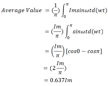
Since two identical diodes are used in center tapped full wave rectifier, the average load current is twice the average load current for half wave rectifier. The average value for full wave rectifier is 0.637 times of the peak current i.e. 0.637Im. Let us now calculate this value. To calculate the average value of load current for full wave rectifier, we assume diode cut-in voltage to be zero. Therefore the load current will start from supply voltage zero and will become zero when supply voltage becomes zero. This is shown below. Blue color shows supply voltage waveform whereas red color shows load current waveform
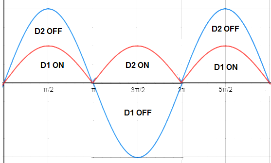
The time period of the load current waveform is π as obvious from the above figure. Thus we can now find the average value by using generalized formula. To know about the generalized formula for average value, you are suggested to read “Average Value of AC Current – Definition, Formula and Application“
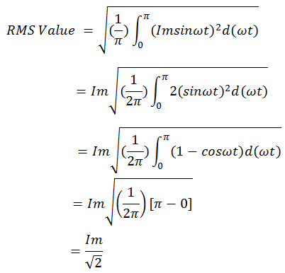
RMS Value of Load Current / Voltage for Full Wave Rectifier
The rms value for full wave rectifier is equal to 0.707 times of peak current i.e. 0.707Im. In fact its rms value is Im/2. Let us now calculate this rms value using generalized formula.
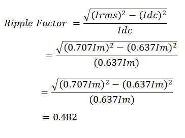
Ripple Factor of Full wave Rectifier
The ripple factor of full wave rectifier is 0.482. If this value is compared with the ripple factor of half wave rectifier (ripple factor 1.21 for half wave), it can be seen that the quality of DC output of full wave rectifier is improved by around 40%. This means the dc output will be smoother and less fluctuating AC component. Let us now derive the ripple factor using formula.
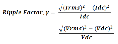
Putting the values of rms current Irms and average current Idc, the value of ripple factor can be calculated.
Form Factor of Full wave Rectifier
Form factor is defined as the ratio of rms value to the average value. For full wave rectifier, we already have calculated the rms current and average current, hence it is quite easy to get the form factor now.
Form Factor = RMS value / Average value
= (0.707Im / 0.637Im)
= 1.11
Thus the form factor of full wave rectifier is equal to 1.11.